- 您现在的位置:买卖IC网 > Sheet目录1994 > DS3231MZ+ (Maxim Integrated Products)IC RTC I2C 8SOIC
±5ppm, I2C Real-Time Clock
2
Maxim Integrated
DS3231M
Stresses beyond those listed under “Absolute Maximum Ratings” may cause permanent damage to the device. These are stress ratings only, and functional
operation of the device at these or any other conditions beyond those indicated in the operational sections of the specifications is not implied. Exposure to absolute
maximum rating conditions for extended periods may affect device reliability.
Voltage Range on Any Pin Relative to GND ........-0.3V to +6.0V
Operating Temperature Range.......................... -45NC to +85NC
Storage Temperature Range............................ -55NC to +125NC
Junction Temperature .....................................................+150NC
Lead Temperature (soldering, 10s) ................................+300NC
Soldering Temperature (reflow) ......................................+260NC
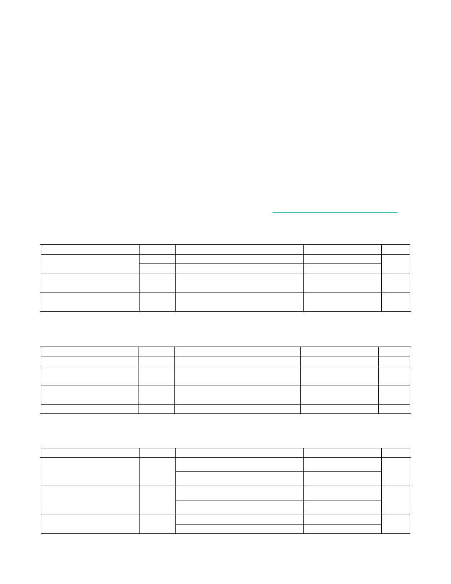
RECOMMENDED OPERATING CONDITIONS
(TA = -45NC to +85NC, unless otherwise noted.) (Note 2)
ELECTRICAL CHARACTERISTICS—FREQUENCY AND TIMEKEEPING
(VCC or VBAT = +3.3V, TA = -45NC to +85NC, unless otherwise noted. Typical values are at VCC = +3.3V, VBAT = +3.0V, and
TA = +25NC, unless otherwise noted.)
DC ELECTRICAL CHARACTERISTICS—GENERAL
(VCC = +2.3V to +5.5V, TA = -45NC to +85NC, unless otherwise noted. Typical values are at VCC = +3.3V, VBAT = +3.0V, and TA =
+25NC, unless otherwise noted.)
ABSOLUTE MAXIMUM RATINGS
8 SO
Junction-to-Ambient Thermal Resistance (
qJA) ........120°C/W
16 SO
Junction-to-Ambient Thermal Resistance (
qJA) ..........90°C/W
Note 1: Package thermal resistances were obtained using the method described in JEDEC specification JESD51-7, using a four-layer
board. For detailed information on package thermal considerations, refer to www.maximintegrated.com/thermal-tutorial.
Package Thermal Characteristics
(Note 1)
PARAMETER
SYMBOL
CONDITIONS
MIN
TYP
MAX
UNITS
Supply Voltage
VCC
2.3
3.3
5.5
V
VBAT
2.3
3.0
5.5
Logic 1
VIH
0.7 x
VCC
VCC +
0.3
V
Logic 0
VIL
-0.3
0.3 x
VCC
V
PARAMETER
SYMBOL
CONDITIONS
MIN
TYP
MAX
UNITS
1Hz Frequency Tolerance
D
f/fOUT
Measured over R 10s interval
Q
5
ppm
1Hz Frequency Stability vs. VCC
Voltage
D
f/V
Q
1
ppm/V
Timekeeping Accuracy
tKA
Q
0.432
Seconds/
Day
32kHz Frequency Tolerance
D
f/fOUT
Q
2.5
%
PARAMETER
SYMBOL
CONDITIONS
MIN
TYP
MAX
UNITS
Active Supply Current
(I2C Active: Includes
Temperature Conversion Current)
ICCA
VCC = +3.63V
200
A
VCC = VCCMAX
300
Standby Supply Current
(I2C Inactive: Includes
Temperature Conversion Current)
ICCS
VCC = +3.63V
130
A
VCC = VCCMAX
200
Temperature Conversion Current
(I2C Inactive)
ICCSCONV
VCC = +3.63V
575
A
VCC = VCCMAX
650
发布紧急采购,3分钟左右您将得到回复。
相关PDF资料
DS3231SN#T&R
IC RTC W/TCXO 16-SOIC
DS3232MZ+
IC RTC W/SRAM I2C 8SOIC
DS3232SN#T&R
IC RTC W/TCXO 20-SOIC
DS3234S#
IC RTC W/TCXO 20-SOIC
DS32C35-33#T&R
IC RTC ACCURATE I2C 3.3V 20-SOIC
DS3911T+
IC DAC 10BIT I2C QUAD 14TDFN
DS4000KI/WBGA
IC OSC TCXO 19.44MHZ 24-BGA
DS4026S+WCN
IC OSC TCXO 25MHZ 16-SOIC
相关代理商/技术参数
DS3231MZ+TRL
功能描述:实时时钟 5+/-ppm RTC RoHS:否 制造商:Microchip Technology 功能:Clock, Calendar. Alarm RTC 总线接口:I2C 日期格式:DW:DM:M:Y 时间格式:HH:MM:SS RTC 存储容量:64 B 电源电压-最大:5.5 V 电源电压-最小:1.8 V 最大工作温度:+ 85 C 最小工作温度: 安装风格:Through Hole 封装 / 箱体:PDIP-8 封装:Tube
DS3231MZEVKIT#
功能描述:时钟和定时器开发工具 Evaluation kit for t he +/-5ppm, I2C Real
RoHS:否 制造商:Texas Instruments 产品:Evaluation Modules 类型:Clock Conditioners 工具用于评估:LMK04100B 频率:122.8 MHz 工作电源电压:3.3 V
DS3231N/DIP
制造商:Rochester Electronics LLC 功能描述: 制造商:Maxim Integrated Products 功能描述:
DS3231S
功能描述:实时时钟 Integrated RTC/TCXO/Crystal RoHS:否 制造商:Microchip Technology 功能:Clock, Calendar. Alarm RTC 总线接口:I2C 日期格式:DW:DM:M:Y 时间格式:HH:MM:SS RTC 存储容量:64 B 电源电压-最大:5.5 V 电源电压-最小:1.8 V 最大工作温度:+ 85 C 最小工作温度: 安装风格:Through Hole 封装 / 箱体:PDIP-8 封装:Tube
DS3231S-
制造商:MAXIM 制造商全称:Maxim Integrated Products 功能描述:Extremely Accurate I2C-Integrated
DS3231S#
功能描述:实时时钟 Integrated RTC/TCXO/Crystal RoHS:否 制造商:Microchip Technology 功能:Clock, Calendar. Alarm RTC 总线接口:I2C 日期格式:DW:DM:M:Y 时间格式:HH:MM:SS RTC 存储容量:64 B 电源电压-最大:5.5 V 电源电压-最小:1.8 V 最大工作温度:+ 85 C 最小工作温度: 安装风格:Through Hole 封装 / 箱体:PDIP-8 封装:Tube
DS3231S#T&R
制造商:Maxim Integrated Products 功能描述:REAL TIME CLOCK SERL 16SOIC W - Tape and Reel 制造商:Maxim Integrated Products 功能描述:REAL TIME CLOCK SERL 16SOIC W - Cut TR (SOS) 制造商:Maxim Integrated Products 功能描述:IC RTC W/TCXO 16-SOIC 制造商:Maxim Integrated Products 功能描述:Real Time Clock Integrated RTC/TCXO/Crystal
DS3231S#T&R
功能描述:实时时钟 Integrated RTC/TCXO/Crystal RoHS:否 制造商:Microchip Technology 功能:Clock, Calendar. Alarm RTC 总线接口:I2C 日期格式:DW:DM:M:Y 时间格式:HH:MM:SS RTC 存储容量:64 B 电源电压-最大:5.5 V 电源电压-最小:1.8 V 最大工作温度:+ 85 C 最小工作温度: 安装风格:Through Hole 封装 / 箱体:PDIP-8 封装:Tube